
2016/01/04

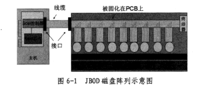
JBOD Interface
Inside JBOD, there is a SCSI bus, which connects all the disks.
Out side of JBOD, there is a SCSI interface, which connects to the host machine.

Out side of JBOD, there is a SCSI interface, which connects to the host machine.
2016/01/01
NVMe Spec Reading Notes
NVM Express is based on a paired Submission and Completion Queue mechanism. Commands are placed by host software into a Submission Queue. Completions are placed into the associated Completion Queue by the controller. Multiple Submission Queues may utilize the same Completion Queue. Submission and Completion Queues are allocated in host memory.
2015/12/25
How MSI-X Works
Explain
There is not interrupt PIN for PCIe interrupt. When device wants to raise an interrupt, an interrupt message is sent to host via inband PCIe channels. The interrupt message is a write command, destination of the write is to the host memory specified by the HOST.
The host specifies the destination address of the interrupt message at the MSI-X table. I believe the MSI-X table is setup by the OS boot up normally.
On X86 platform, the interrupt message is written to LAPIC (Local component of Advanced Programmable Interrupt Controller ), usually integrated into the processor itself.
On ARM platform, the interrupt message is written to ARM Generic Interrupt Controller(GIC), GIC's LPI (Locality-specific Peripheral Interrupts) and ITS(Interrupt Translation Service) support MSI-X messages.

Reference
http://www.alterawiki.com/wiki/Implementing_MSI-X_for_PCI_Express_in_Altera_FPGA_Devices
https://en.wikipedia.org/wiki/PCI_configuration_space
http://www.slideshare.net/anshumanbiswal/cjb0412001-anshumanaspesd2528presentation
https://en.wikipedia.org/w/index.php?title=Advanced_Programmable_Interrupt_Controller&redirect=no
Quotes
--------------
6.8.2. MSI-X Capability & Table Structures
In contrast to the MSI capability structure, which contains Message Address and Message
Data registers, the MSI-X capability structure contains a BAR Indicator register (BIR) and
Table Offset register. The separate MSI-X Table structure typically contains multiple
entries, each consisting of a Message Address field and Message Data field, and thus capable
of specifying a unique vector. The MSI-X Table is mapped by the Base Address register
indicated by the BIR, which refers to one of the function’s Base Address registers located
beginning at 10h in Configuration Space. The indicated Base Address register may be either
32-bit or 64-bit, but must map Memory Space.
Compared to the MSI capability structure, the MSI-X capability structure does not contain all controls and status information. The MSI-X capability structure instead points to a MSI-X Table structure and a MSI-X Pending Bit Array (PBA) structure, both of them reside in the device’s memory space. Each structure is mapped to the device’s memory space by a PCIe BAR which is located beginning at offset 10h in the Configuration Space.
The Table BIR (BAR Indicator Reigster) and PBA BIR in the MSI-X capability structure indicates which PCIe BAR the structure is mapped to. For example, if the value in BIR is 0, it means the structure is mapped through PCIe Bar0 at offset 10h in the Configuration Space. If the value in BIR is 1, it means the structure is mapped through PCIe Bar1 and so on. The BAR is permitted to be either 32-bit or 64-bit, but the BAR must be memory mapped, not mapped to IO space. The two structures can be mapped to the same BAR or two different BARs.
The Offset is QWORD-aligned and indicates where the structure begins relative to the base address associated with the BAR.
The MSI-X Table Structure contains multiple entries and eachentry represents one interrupt vector. Each entry has 4 QWORDs and consists of a32-bit lower Message Address, 32-bit upper Message Address, 32-bit data, and asingle Mask bit in the Vector Control field as shown in Figure 4 below. When the device wants to transmit a MSI-X interrupt message, it does
Picks up an entry in the Table Structure, sendsout a PCIe memory write with the address and data in the table to the system host.
Sets the associated bit in the PBA structure to represent which MSI-X is prepared to be sent and the bit is set before MSI-X interrupt is sent. The bit is set when the corresponding MSI-X vector is masked, it means there is MSI-X is pending, the message is not sent out because the vector is masked. When the vector is unmasked, the message is out and the PBA bit is cleared.
After the MSI-X message is sent, the function which generates the MSI-X interrupt clears the bit.
The APIC is a split architecture design, with a local component (LAPIC) usually integrated into the processor itself, and an optional I/O APIC on a system bus
The Message Signaled Interrupts (MSI) feature of the PCI 2.2 and later specifications cannot be used without the local APIC being enabled.[8] Use of MSI obviates the need for an I/O APIC. Additionally, up to 224 interrupts are supported in MSI mode, and IRQ sharing is not allowed.
There is not interrupt PIN for PCIe interrupt. When device wants to raise an interrupt, an interrupt message is sent to host via inband PCIe channels. The interrupt message is a write command, destination of the write is to the host memory specified by the HOST.
The host specifies the destination address of the interrupt message at the MSI-X table. I believe the MSI-X table is setup by the OS boot up normally.
On X86 platform, the interrupt message is written to LAPIC (Local component of Advanced Programmable Interrupt Controller ), usually integrated into the processor itself.
On ARM platform, the interrupt message is written to ARM Generic Interrupt Controller(GIC), GIC's LPI (Locality-specific Peripheral Interrupts) and ITS(Interrupt Translation Service) support MSI-X messages.

Reference
http://www.alterawiki.com/wiki/Implementing_MSI-X_for_PCI_Express_in_Altera_FPGA_Devices
https://en.wikipedia.org/wiki/PCI_configuration_space
http://www.slideshare.net/anshumanbiswal/cjb0412001-anshumanaspesd2528presentation
https://en.wikipedia.org/w/index.php?title=Advanced_Programmable_Interrupt_Controller&redirect=no
Quotes
--------------
6.8.2. MSI-X Capability & Table Structures
In contrast to the MSI capability structure, which contains Message Address and Message
Data registers, the MSI-X capability structure contains a BAR Indicator register (BIR) and
Table Offset register. The separate MSI-X Table structure typically contains multiple
entries, each consisting of a Message Address field and Message Data field, and thus capable
of specifying a unique vector. The MSI-X Table is mapped by the Base Address register
indicated by the BIR, which refers to one of the function’s Base Address registers located
beginning at 10h in Configuration Space. The indicated Base Address register may be either
32-bit or 64-bit, but must map Memory Space.
Compared to the MSI capability structure, the MSI-X capability structure does not contain all controls and status information. The MSI-X capability structure instead points to a MSI-X Table structure and a MSI-X Pending Bit Array (PBA) structure, both of them reside in the device’s memory space. Each structure is mapped to the device’s memory space by a PCIe BAR which is located beginning at offset 10h in the Configuration Space.
The Table BIR (BAR Indicator Reigster) and PBA BIR in the MSI-X capability structure indicates which PCIe BAR the structure is mapped to. For example, if the value in BIR is 0, it means the structure is mapped through PCIe Bar0 at offset 10h in the Configuration Space. If the value in BIR is 1, it means the structure is mapped through PCIe Bar1 and so on. The BAR is permitted to be either 32-bit or 64-bit, but the BAR must be memory mapped, not mapped to IO space. The two structures can be mapped to the same BAR or two different BARs.
The Offset is QWORD-aligned and indicates where the structure begins relative to the base address associated with the BAR.
The MSI-X Table Structure contains multiple entries and eachentry represents one interrupt vector. Each entry has 4 QWORDs and consists of a32-bit lower Message Address, 32-bit upper Message Address, 32-bit data, and asingle Mask bit in the Vector Control field as shown in Figure 4 below. When the device wants to transmit a MSI-X interrupt message, it does
Picks up an entry in the Table Structure, sendsout a PCIe memory write with the address and data in the table to the system host.
Sets the associated bit in the PBA structure to represent which MSI-X is prepared to be sent and the bit is set before MSI-X interrupt is sent. The bit is set when the corresponding MSI-X vector is masked, it means there is MSI-X is pending, the message is not sent out because the vector is masked. When the vector is unmasked, the message is out and the PBA bit is cleared.
After the MSI-X message is sent, the function which generates the MSI-X interrupt clears the bit.
The APIC is a split architecture design, with a local component (LAPIC) usually integrated into the processor itself, and an optional I/O APIC on a system bus
The Message Signaled Interrupts (MSI) feature of the PCI 2.2 and later specifications cannot be used without the local APIC being enabled.[8] Use of MSI obviates the need for an I/O APIC. Additionally, up to 224 interrupts are supported in MSI mode, and IRQ sharing is not allowed.
2015/11/13
Direct IO
Need to find out how kernel can direct read write user space memory.
sg_io()
blk_rq_map_user_iov() in block/blk-map.c worth a check.
bio_map_user_iov()
sg_io()
blk_rq_map_user_iov() in block/blk-map.c worth a check.
bio_map_user_iov()
2015/10/18
MLC Page Written Randomly?
Can UBI logical eraseblocks be written randomly?
No, the flash chip restrictions have to be taken into account. This is because UBI logical eraseblocks (LEB) are mapped to physical eraseblocks (PEB), and an LEB write operation is essentially a write to the corresponding PEB plus a small offset. The important flash restrictions are:
all writes have to be aligned to the min. I/O unit size and be multiple of min. I/O unit size;
sometimes it is prohibited to write more then once to the same PEB offset (e.g., in case of NAND flash);
many NAND flashes (specifically, MLC NAND flashes) require NAND pages to be written sequentially from the beginning of the physical eraseblock, to the end of the physical eraseblock; for example, it is prohibited to first write to offset 2048, then to offset 0; once offset 2048 has been written to, it is possible to write only to further offsets.
Even if the flash chip is devoid of the last restriction, UBI anyway requires logical eraseblocks to be written sequentially from the beginning to the end. This is because UBI calculates data CRC when moving logical eraseblocks to other physical eraseblocks (see here for more information), so a write an offset which is less than the furthest written data offset causes CRC errors;
Reference
http://www.linux-mtd.infradead.org/faq/ubi.html
No, the flash chip restrictions have to be taken into account. This is because UBI logical eraseblocks (LEB) are mapped to physical eraseblocks (PEB), and an LEB write operation is essentially a write to the corresponding PEB plus a small offset. The important flash restrictions are:
all writes have to be aligned to the min. I/O unit size and be multiple of min. I/O unit size;
sometimes it is prohibited to write more then once to the same PEB offset (e.g., in case of NAND flash);
many NAND flashes (specifically, MLC NAND flashes) require NAND pages to be written sequentially from the beginning of the physical eraseblock, to the end of the physical eraseblock; for example, it is prohibited to first write to offset 2048, then to offset 0; once offset 2048 has been written to, it is possible to write only to further offsets.
Even if the flash chip is devoid of the last restriction, UBI anyway requires logical eraseblocks to be written sequentially from the beginning to the end. This is because UBI calculates data CRC when moving logical eraseblocks to other physical eraseblocks (see here for more information), so a write an offset which is less than the furthest written data offset causes CRC errors;
Reference
http://www.linux-mtd.infradead.org/faq/ubi.html
2015/10/12
Linux Support for eMMC
Software Layer
File System (Sector Based)
Card (Block Device Driver)
Core (eMMC Driver )
Host (Host Driver, Platform Dependent)
eMMC Card (Card)
The eMMC subsystem (./drivers/mmc) is organized into three layers:
• The card layer is the external interface. It is seen as a block device driver, depending
on the enablement of block layer support for the kernel and interfaces within the file
system.
• The core layer implements all eMMC-dependent functionality, such as main operations,
command management, host setting, management functions, and high-level
functions.
• The host layer implements the driver for most known platform controllers and is platform
dependent.
SDHCI Specification
https://www.sdcard.org/downloads/pls/partA2_300.pdf
Reference
https://www.sdcard.org/downloads/pls/partA2_300.pdf
http://www.ebv.com/fileadmin/design_solutions/php/download.php?path=fileadmin%2Fproducts%2FEBVuniversity%2F120912_Micron_e.MMC%2F120912_mic_emmc_Linux.pdf
File System (Sector Based)
Card (Block Device Driver)
Core (eMMC Driver )
Host (Host Driver, Platform Dependent)
eMMC Card (Card)
The eMMC subsystem (./drivers/mmc) is organized into three layers:
• The card layer is the external interface. It is seen as a block device driver, depending
on the enablement of block layer support for the kernel and interfaces within the file
system.
• The core layer implements all eMMC-dependent functionality, such as main operations,
command management, host setting, management functions, and high-level
functions.
• The host layer implements the driver for most known platform controllers and is platform
dependent.
SDHCI Specification
https://www.sdcard.org/downloads/pls/partA2_300.pdf
Reference
https://www.sdcard.org/downloads/pls/partA2_300.pdf
http://www.ebv.com/fileadmin/design_solutions/php/download.php?path=fileadmin%2Fproducts%2FEBVuniversity%2F120912_Micron_e.MMC%2F120912_mic_emmc_Linux.pdf
Subscribe to:
Posts (Atom)
-
 Explain There is not interrupt PIN for PCIe interrupt. When device wants to raise an interrupt, an interrupt message is sent to host via ...
 -
 Configure Space Addressing One of the major improvements the PCI Local Bus had over other I/O architectures was its configuration mechanism...
 -
Example goes here: String url3 = " https://ajax.googleapis.com/ajax/services/search/news?v=1.0&q=barack%20obama " ; JsonpR...